
[Necessary for circuit designers] MOS tube parameters detailed and accurate selection
2024-05-07 13:54:59
The MOS tube is a metal-oxide-semiconductor field-effect transistor, which is a Semiconductor device that works using the field-effect principle.
Compared with ordinary bipolar transistors, MOS transistors have the advantages of high input impedance, low noise, large dynamic range, low power consumption, easy integration, etc., and have been more and more widely used in the field of high-frequency power supplies such as switching power supplies, ballasts, high-frequency induction heating, high-frequency inverter welding machines, and communication power supplies.
Field effect tube classification
There are two types of Fets: junction type (JFET) and metal-oxide-semiconductor type (MOSFET).
The full English name of JFET is Junction Field-Effect Transistor, which is also divided into N channel and P channel, and is almost not used in practice.
The English full name of MOSFET is Metal-Oxide-Semiconductor Field-Effect Transistor, which is widely used, and MOSFET is generally called MOS tube.
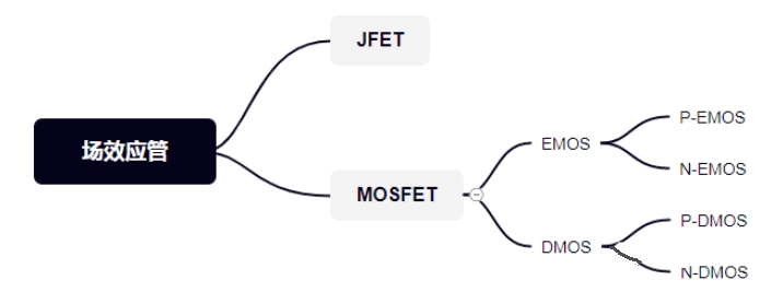
MOS tube is a kind of FET (the other is JFET junction FET), which has two main structural forms: N-channel type and P-channel type.
According to the different principle of field effect, it is divided into two types: depletion type (when the gate voltage is zero, there is a larger drain current) and enhanced type (when the gate voltage is zero, the drain current is also zero, and a certain gate voltage must be added before there is a drain current).
Therefore, MOS tubes can be made into four types of products: P-channel enhanced, P-channel depleted, N-channel enhanced and N-channel depleted.
Generally, the most used on the motherboard is the enhanced MOS tube, NMOS is the most, generally used in signal control, followed by PMOS, used in power switches and other aspects, and the depletion type is almost not used.
N and P distinguish
Each MOS tube is provided with three electrodes: the Gate gate (represented by "G"), the Source source (represented by "S"), and the Drain drain (represented by "D"). When wiring, the power input of channel N is D and the output is S; The power input of the P channel is S and the output is D; And the connection method of enhanced and depleted type is basically the same.

The red arrow pointing to the G pole is NMOS, and the arrow pointing back to the G pole is PMOS
Parasitic diode
Due to the production process, the general MOS tube will have a parasitic diode, and some are also called body diodes.
 Those marked in red are volume diodes
It can be seen from the above figure that the directions of NMOS and PMOS parasitic diodes are different, NMOS is from the S pole to the D pole, and PMOS is from the D pole to the S pole.
The parasitic diode is the same as the ordinary diode, the positive connection will be on, and the reverse connection will be off. For NMOS, when the S pole is positive and the D pole is negative, the parasitic diode will be on, and the reverse connection will be off. For PMOS, when the D pole is connected to the positive, the S pole is connected to the negative, the parasitic diode is on, and the reverse is off.
In some applications, the body diode will also be chosen to reduce the voltage drop between DS (the pressure drop of the body diode is much larger than the on-off voltage drop of the MOS), and the overcurrent capacity of the body diode should also be concerned.
When the on-condition of the MOS tube is met, the D pole and S pole of the MOS tube will be on, and the body diode is off at this time, because the on-resistance of the MOS tube is very small, the general mΩ level, the current flowing through the 1A level, is also mV level, so the on-voltage drop between the D pole and the S pole is very small, not enough to make the parasitic diode on-, which needs special attention.
Working principle of MOS tube (Taking N-channel enhanced type as an example)
The N-channel enhanced MOS tube generates a SiO2 thin film insulation layer on the P-type semiconductor, and then diffuses two highly doped N-type regions by photolithography process, from which electrodes (drain D, source S) are extracted. A layer of metal aluminum is plated on the SiO2 insulation layer between the source and drain as the gate G; P-type semiconductors are called substrates and are represented by the symbol B. Because the gate and other electrodes are insulated from each other, NMOS is also called an insulated gate type field effect tube.
When no voltage is added between the gate G and the source S, that is, VGS=0, due to the P-type substrate between the drain and the source two N+ areas, which is equivalent to two back-to-back PN junctions, the resistance between them is as high as 1012Ω, that is, there is no conductive channel between D and S, so no matter what polarity voltage is added between the drain and the source, No drain current ID is generated.
 N channel enhanced MOS tube structure diagram
When the substrate B is short-circuited with the source S and a positive voltage is applied between the gate G and the source S, i.e., VGS > 0, as shown in the figure above, an electric field is generated between the gate and the substrate from the gate towards the substrate. Under the action of this electric field, the holes near the P substrate surface are repelled and will move downward, and the electrons are attracted by the electric field to move towards the substrate surface, and compound with the holes on the substrate surface to form a depletion layer.
If the VGS voltage is further increased, so that the VGS reaches a certain voltage VT, all the holes in the P substrate surface layer are repelled and exhausted, and a large number of free electrons are attracted to the surface layer, from quantitative change to qualitative change, so that the surface layer becomes a free electron for many sons of the N-type layer, called the "inverse layer", as shown in the figure below.
The inverse layer connects the two N+ type regions of the drain D and the source S, forming the N-type conductive channel between the drain and the source. The VGS value required to start forming a conductive channel is called the threshold voltage or the opening voltage and is represented by VGS (th). Obviously, there is a channel only when VGS > VGS (th), and the larger the VGS, the thicker the channel, the smaller the on-resistance and the stronger the conductivity of the channel. Hence the term "enhanced".
 Schematic diagram of the structure generated by depletion layer and inversion layer
Under the condition of VGS > VGS (th), if the positive voltage VDS is added between the drain D and the source S, there will be current flow in the conductive channel. The drain current flows from the drain region to the source region. Because there is a certain resistance in the channel, a voltage drop is generated along the channel, making the potential of each point in the channel gradually decrease from the drain region to the source region along the channel. The voltage near the end of the drain region is VGD, whose value is VGD=VGS-VDS, and the corresponding channel is the thinest. The voltage near the source area is the largest, equal to VGS, and the corresponding channel is the thickest.
This makes the channel thickness is no longer uniform, and the entire channel is inclined. With the increase of VDS, the channel near the leakage zone becomes thinner and thinner.
When VDS increases to a certain critical value, making VGD≤VGS (th), the channel at the drain end disappears, leaving only the depletion layer, which is called the channel "pre-pinch", as shown in Figure (a) below. Continue to increase VDS[that is, VDS > VGS-VGS (th)], and the clip breakpoint moves towards the source, as shown in Figure (b) below.
Although the pinch point is moving, the voltage drop in the channel region (source S to the pinch point) remains the same and is still equal to VGS-VGS (th). Therefore, the excess voltage of VDS [VDS- (VGS-VGS (th))] is all reduced to the pinch zone, and a strong electric field is formed in the pinch zone. At this time, the electrons flow from the source to the pinch zone along the channel. When the electrons reach the edge of the pinch zone, they will quickly drift to the drain due to the strong electric field in the pinch zone.
 Schematic diagram of pre-clamping and clamping zone formation
Conduction condition
The MOS tube is voltage controlled, and the conduction is determined by the pressure difference between the G and S poles.
For NMOS, Vg-Vs>Vgs(th), that is, the pressure difference between the G pole and the S pole is greater than a certain value, the MOS tube will be on, but it cannot be too large, otherwise the MOS tube will be burned, and the opening voltage and other parameters can be seen by the SPEC of the specific device.
For PMOS, Vs-Vg>Vgs(th), that is, the pressure difference between the S pole and the G pole is greater than a certain value, the MOS tube will be on, similarly, the specific parameters refer to the SPEC of the device.
Triode is current control, MOS tube is voltage control, the main differences are as follows:
1, only allow to take a small amount of current from the signal source, select the MOS tube; Under the condition that the signal voltage is low and more current is allowed from the signal source, the triode is selected.
2, the MOS tube is a unipolar device (by a majority of carriers conducting), the transistor is a bipolar device (both a majority of carriers, but also a minority of carriers conducting).
3, the source and drain of some MOS tubes can be used interchangeably, the grid can also be positive or negative, and the flexibility is better than the transistor.
4. MOS tube is widely used and can work under very small current and very low voltage.
5, MOS tube input impedance is large, low noise, MOS tube is more expensive, triode loss.
6, MOS tube is commonly used as a power switch, as well as large current switching circuit, high-frequency high-speed circuit, transistor is commonly used to digital circuit switch control.
The role of series resistance of G and S poles
The input impedance of the MOS tube is very large, easy to be interfered by external signals, as long as a small amount of static electricity, it can make the equivalent capacitance between the G-S electrode at both ends of the high voltage, if not timely release of static electricity, the high voltage at both ends is easy to make the MOS tube produce misoperation, and even may breakdown the G-S pole, play a fixed level role.
The role of G pole series resistance
MOS tubes are voltage-controlled, and in some cases, why do you need a resistor in series at the G pole?
1. Slow down Rds from infinity to Rds(on).
2, to prevent vibration, the general single chip microcomputer I/O output will have a point of stray inductance, in the case of voltage mutation, may form LC oscillation with the gate capacitor, series resistance can increase the damping and reduce the oscillation effect.
3, reduce the peak grid charging current.
Key points of selection
1. Voltage value
Pay attention to the maximum on-voltage of Vds and the maximum withstand voltage of Vgs. In actual use, this value cannot be exceeded, otherwise the MOS tube will be damaged.
 Pay attention to the on-voltage Vgs(th), the MOS tube is generally controlled by a single chip microcomputer, and the MOS tube with an appropriate on-threshold value is selected according to the level of the GPIO of the single chip microcomputer, and a certain margin is left as far as possible to ensure that the MOS can be switched normally.
 2. Current value
Pay attention to the ID current, this value represents how much current the NMOS tube can flow and the ability to react with load, beyond this value, the MOS tube will also be damaged.
 3. Power loss
Power loss needs to pay attention to the following parameters, including thermal resistance and temperature. Thermal resistance refers to the ratio between the temperature difference at both ends of the object and the power of the heat source when heat is transmitted on the object, the unit is ° C /W or K/W, and the formula of thermal resistance is ThetaJA = (Tj-Ta)/P, which is related to power and ambient temperature.
 4. Conducting the internal resistance
The conduction internal resistance pays attention to the Rds(on) parameter of NMOS. The smaller the conduction internal resistance, the smaller the loss of NMOS tube. Generally, the conduction internal resistance of NMOS tube is at the mΩ level.
5. Switch time
MOS as a switching device, there will be a switching time concept, in the high-speed circuit, as far as possible to choose the input and output capacitance Ciss&Coss small, the switching time Ton&Toff short MOS tube, to ensure normal data communication.
6. Packaging
According to the size of the PCB board, choose the appropriate NMOS tube size, in the case of limited on-board area, choose as small package as possible; Try to choose a common package, in order to prepare for the subsequent selection of suitable alternative materials.


