Buck circuit principle analysis and device selection skills
2024-05-08 14:34:46
Buck circuit, also known as buck circuit, is a common DC-DC converter whose function is to convert the input DC voltage to a DC voltage lower than the input voltage. It is one of the most basic topologies in non-isolated DC converters and is widely used in battery-powered devices, power adapters, LED drivers and other fields to achieve efficient and stable voltage conversion.
Buck circuit working principle
The basic structure of the Buck circuit consists of a switch (usually a MOSFET), an energy storage inductor L, a filter capacitor C, and a load resistor. The operation of the circuit is based on the high frequency switch on and off, with the filter characteristics of inductors and capacitors, to achieve voltage conversion.
When the power supply is closed, the voltage will increase rapidly, when the voltage will decrease rapidly, if the switching speed is fast enough, is it possible to control the load within the desired voltage value?
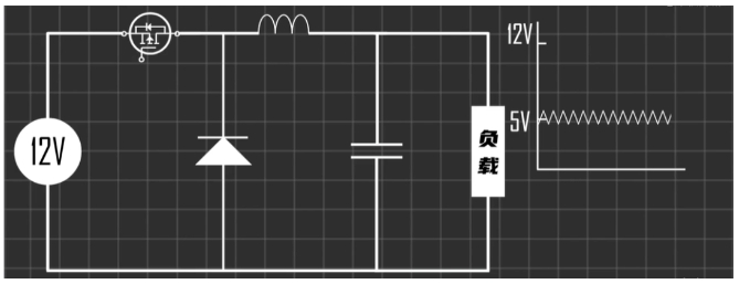 Assuming the 12V step-down to 5V, it means that the MOS tube switch needs to be on 42% of the time and off 58% of the time.
When the MOS tube is on 42% of the time, the inductance is magnetized to store energy, and the capacitor is charged to provide power to the load.
When the MOS tube is disconnected 58% of the time, because the current on the inductor cannot change, the circuit supplies power to the load through the current and capacitance of the inductor, thus maintaining the voltage at the load end at 5V.
Control mode: The output voltage of the Buck circuit can be controlled by adjusting the duty cycle of the switch (that is, the ratio of the switch on time to the total cycle in a switching cycle). The higher the duty cycle, the closer the output voltage is to the input voltage but does not exceed the input voltage. Otherwise, the output voltage is lower. Working mode:
- Continuous conduction mode (CCM) : During each switching cycle, the inductive current is always greater than zero and continues to flow.
- Discontinuous conduction mode (DCM) : During certain switching cycles, the inductive current drops to zero and is discontinuous.
- Boundary conduction mode (BCM) : A special case in which the inductive current drops exactly to zero at the end of each cycle.
Device selection of Buck circuit
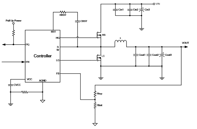
Buck circuit mainly consists of the following parts:
-
Controller chip: responsible for generating control signals to drive the power switch, adjust the duty ratio according to the preset algorithm or external control signals to maintain the stability of the output voltage.
-
Power MOS (such as MOSFET) : as a switching component in the circuit, it is switched on or off according to the signal of the controller, controlling the transmission of electrical energy.
-
Power inductance: store and release energy in the circuit, when the power MOS tube is on, the inductance current rises, and the energy is stored; When the MOS tube is turned off, the inductor releases energy through the diode (or a second MOSFET in a synchronous Buck circuit) toward the load while maintaining a continuous current.
-
Input/output filter capacitor: The input filter capacitor is used to smooth the input voltage and filter the ripple, and the output filter capacitor further filters the ripple of the output voltage to ensure the stability and high quality of the output DC voltage.
Selection of controller chip
According to the actual application scenario, the controller must first meet the technical parameters of the switching power supply circuit, then meet the working environment requirements of the circuit, and finally choose the suitable power supply scheme within the cost control range.
Analog or digital controller: Digital controllers have simple peripheral circuits, are easier to debug online, and can be flexibly configured according to the application.
Single phase or polyphase: Select the number of phases according to the output current. If the number of phases is not enough, it can not meet the current demand, and if the number of phases is too much, the cost will increase. Output current below 30A, choose a single-phase controller; More than 30A is increased to 2 phases, and so on, generally maintain each phase current in the range of 15A~30A (depending on the capacity of the power device) is more reasonable.
Input and output voltage range: Select a controller chip with appropriate input and output voltages according to the actual application scenario to ensure that the input voltage is within the acceptable range of the control and that the output voltage size and accuracy meet the requirements of the circuit design.
Communication protocols: For digital controllers, it is necessary to consider which communication protocols are supported by the controller chip to meet the allocation of communication interfaces by the master chip.
Selection of power MOS tube
Vds voltage resistance: Ensure that the pressure difference between the two ends of the actual MOS tube is less than the Vds voltage resistance, to avoid the MOS tube breakdown. Considering that the waveforms at both ends of the MOS tube DS will ring when the circuit is actually working, the Vds voltage is generally selected to be more than 10V higher than the input voltage, such as the input 20V, the MOS with a Vds voltage of 30V is selected.
Id current: Ensure that the peak output current does not exceed Id, which can be judged by the SOA curve of the MOS tube. The Id current indicated in the MOS specification is calculated based on Rdson and maximum power Pd, without considering the switching loss, so it cannot be directly compared with the Irms of MOS, and the overall loss of MOS needs to be calculated to determine the selection.
Rdson and Qg: These two parameters affect the loss of the MOS tube. The principle is that the MOS tube with lower Qg is selected for the upper tube, and the MOS with smaller Rdson is selected for the lower tube. If the duty cycle of the PWM of the Buck circuit is large (> 50%), the on-off loss of the upper tube can not be ignored, and both Qg and Rdson parameters are required to be small. In addition, the switching loss can be reduced by reducing the switching frequency of the MOS tube or by connecting the MOS tube in parallel.
Power inductor selection
Inductance value: Inductance value can be calculated using the following formula, where r is the current ripple rate, generally choose about 0.3~0.5:
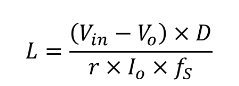 The value will affect the ripple and dynamic response of the output power supply, and should be adjusted according to the actual test results.
Current: The current of the inductor is divided into saturation current Isat and temperature rise current Irms. The current waveform on the inductor during actual operation is as follows:
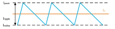 When selecting inductors, first of all, it is necessary to ensure that the saturation current Isat is greater than the peak inductance current Ipeak, so as to avoid inductance saturation, and the induction value drop will cause MOS and inductance damage.
The temperature rise current is from the perspective of the operating temperature and loss of the inductor, and the temperature rise current should be greater than the effective value of the inductor current as far as possible during selection, as shown in the following formula:
 DCR (DC resistance) : If the power circuit uses inductor DCR for current detection, in order to ensure the consistency of the detection results, the DCR accuracy of the inductor should be selected as far as possible within ±5%.
Filter capacitor selection
The selection of filter capacitors requires consideration of a number of factors, including but not limited to the operating frequency, load characteristics, the frequency range of noise required to be filtered, the space limitations of the circuit, the cost, and the physical characteristics of the capacitor. The following are some basic selection guidelines: Determine the application needs: Frequency range: Low frequency applications (such as 50/60Hz power frequency) usually use high-capacity electrolytic capacitors because they are better able to filter out low frequency ripple. High frequency applications (such as hundreds of kHz to MHz in switching power supplies) tend to use ceramic capacitors because they have low equivalent series resistance (ESR) and equivalent series inductance (ESL), which are suitable for filtering out high-frequency noise. Bulk reactance calculation: Calculate the required bulk reactance (Xc = 1/(2πfC)), where f is the frequency and C is the capacitance value. In general, the capacitive reactance of the filter capacitor should be about 1/15 of the load resistance to effectively filter out the clutter of the fundamental frequency.
Voltage withstand value: The voltage withstand of the general capacitor needs to be derated to about 90%. For higher reliability, the derated value is required to 50% in some specific scenarios.
Capacitance value: The capacitance value of the capacitor affects the effect of filtering and voltage regulation, theoretically the larger the capacitance value, the better the effect.
Type selection:
-
Electrolytic capacitors are suitable for applications that require large capacities, but have large ESR and ESL, and have a limited life.
-
Ceramic capacitors are used for high-frequency filtering and have low ESR and ESL, but relatively small capacity.
-
Thin film capacitors are used in some high-performance applications, where they have low ESR, stable temperature characteristics, but at a higher cost.
PCB Layout:
Capacitors should be placed as close to the load as possible to reduce the effect of lead inductance. For high-frequency filtering, the ground foot of the capacitor should be as close to the ground plane as possible.
Actual test and adjustment:
After the initial selection, the actual application may need to optimize the configuration of the capacitor through testing and adjustment to ensure that the desired filtering effect is achieved.
In fact, the frequency-impedance characteristic curve of the capacitor is not linear, and the characteristic curve of different capacitors is different. As shown in the figure below, the characteristic curves of 330uF, 22uF and 0.1uF are respectively.
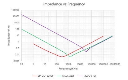
In the low frequency band, the impedance of 330uF is significantly lower than that of 22uF and 0.1uF, in the middle frequency band, the impedance of 22uF is lower, and the impedance of high frequency band 0.1uF is lower. Therefore, it is necessary to select capacitive combined filtering with different capacitance values for power supply noise in different frequency bands.
In the input and output of Buck circuit, the combination of solid-state electrolytic capacitor with large capacity and MLCC with small capacity is generally selected to achieve low impedance in all frequency bands.
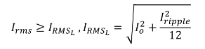
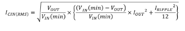
Maximum ripple current: The effective value of the capacitor ripple current is greater than the actual input capacitor ripple current. The effective value of the input capacitance ripple current can be calculated according to the following formula:
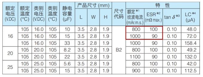
 ESR (Equivalent Series resistance) : The ESR of the capacitor mainly affects the ripple of the power supply and is also related to the ripple current RMS of the capacitor. In general, the smaller the ESR of the capacitor, the larger the ripple current RMS value, as shown in the figure below: